CCD Signal-To-Noise Ratio
For any electronic measuring system, the signal-to-noise ratio (SNR) characterizes the quality of a measurement and determines the ultimate performance of the system. Many digital cameras for microscopy utilize a CCD (charge-coupled device) image sensor, the SNR value specifically represents the ratio of the measured light signal to the combined noise, which consists of undesirable signal components arising in the electronic system, and inherent natural variation of the incident photon flux. Because a CCD sensor collects charge over an array of discrete physical locations, the signal-to-noise ratio may be thought of as the relative signal magnitude, compared to the measurement uncertainty, on a per-pixel basis. The three primary sources of noise in a CCD imaging system are photon noise, dark noise, and read noise, all of which must be considered in the SNR calculation.
The tutorial initializes with the display of a graphical plot of signal-to-noise ratio as a function of integration (exposure) time for a hypothetical CCD system with specifications typical of high-performance cameras used in microscopy imaging applications. Parameters that affect signal-to-noise ratio for a CCD sensor can be varied for the system modeled in the tutorial by using the mouse to reposition any of the sliders located below the display window. As each variable is changed, the calculated value of signal-to-noise ratio is updated in the left-hand yellow box. During image acquisition with electronic sensors, including CCDs, apparently random fluctuations in signal intensity constitute noise superimposed on the signal, and as the magnitude of noise increases, uncertainty in the measured signal becomes greater. Changes made to the factors that directly affect signal level, and to those variables primarily contributing noise to the system, have an inverse effect on SNR that is reflected in the displayed value. A large signal-to-noise ratio is important in the acquisition of high-quality digital images, and is particularly critical in applications requiring precise light measurements. The radio buttons labeled Binning Factor can be selected individually to enable a method of signal-to-noise ratio improvement commonly used with scientific CCD cameras, in which the signal-generated charge from groups of neighboring pixels is combined during readout into larger "superpixels". The binning factor represents the number of pixels that are combined to form each larger pixel. When the SNR is recalculated to reflect the binning operation, it is assumed that the signal is the same for each pixel within a group.
The measured signal from a CCD imaging system, utilized in calculating SNR, depends upon the photon flux incident on the CCD (expressed as photons per pixel per second), the quantum efficiency of the device (where 1 represents 100 percent efficiency), and the integration (exposure) time over which the signal is collected (seconds). The product of these three variables determines the signal portion (numerator) of the signal-to-noise ratio, which is weighed against all noise sources that contribute to the denominator term of the ratio. TheQuantum Efficiency slider in the tutorial provides an adjustment range of 20 to 98 percent, and the Photon Flux slider allows selecting incident light levels between 0.1 and 10000 photons per pixel per second. The Integration Time slider adjusts the CCD integration time over a range of 0.1 to 100 seconds.
Sliders are provided for varying the CCD specifications for Read Noise (2 to 20 electrons rms per pixel) and for Dark Current (0.01 to 50 electrons per pixel per second). The photon noise contribution to total noise is a function of signal level and is not an independent noise variable that can be reduced through camera design or method of operation, but is accounted for in the SNR calculation. The right-hand yellow numerical field (Detected Photons/Pixel) displays the total number of signal photons read out by the CCD for each pixel over the integration period currently set by the slider. This value represents the product of photon flux, quantum efficiency, and integration time. Manipulation of the five sliders, in conjunction with the radio buttons adjacent to several, produces a range of signal-to-noise ratio values corresponding to most operating conditions likely to be encountered in the use of CCD cameras designed for low light imaging in microscopy. When the tutorial is initially loaded or is reset, the slider positions default to values that are typical for a high-performance scientific grade camera system utilizing a cooled CCD.
Three primary undesirable signal components (noise), which degrade the performance of a CCD imaging device by lowering signal-to-noise ratio, are considered in calculating overall SNR:
Photon noise (sometimes referred to as shot noise) results from the inherent statistical variation in the arrival rate of photons incident on the CCD. Photoelectrons generated within the semiconductor device constitute the signal, the magnitude of which is perturbed by fluctuations that follow the Poisson statistical distribution of photons incident on the CCD at a given location. The photon noise, or measurement variation, is therefore equivalent to the square-root of the signal.
Dark noise arises from statistical variation in the number of electrons thermally generated within the silicon structure of the CCD, which is independent of photon-induced signal, but highly dependent on device temperature. The rate of generation of thermal electrons at a given CCD temperature is termed dark current. In similarity to photon noise, dark noise follows a Poisson relationship to dark current, and is equivalent to the square-root of the number of thermal electrons generated within the image exposure time. Cooling the CCD reduces the dark current dramatically, and in practice, high-performance cameras are usually cooled to a temperature at which dark current is negligible over a typical exposure interval.
Read noise is a combination of system noise components inherent to the process of converting CCD charge carriers into a voltage signal for quantification, and the subsequent processing and analog-to-digital conversion. The major contribution to read noise usually originates with the on-chip preamplifier, and this noise is added uniformly to every image pixel. High-performance camera systems utilize design enhancements that greatly reduce the significance of read noise.
The CCD signal-to-noise ratio calculation in the tutorial uses the following equation:
Formula 1 - Signal-to-Noise Ratio
SNR = PQet / [ PQet + Dt + Nr2 ]1/2
An additional factor that should be considered is that the values of incident and background photon flux, and quantum efficiency are functions of wavelength, and when broadband illumination sources are employed, the calculation of signal-to-noise ratio requires these variables to be integrated over all wavelengths utilized for imaging.
Various approaches are used to increase signal-to-noise ratio in high-performance CCD imaging systems. To reduce thermal charge generation within the semiconductor layers of the CCD, which is manifested as dark current, special device fabrication techniques and operation modes are sometimes employed. It is common to cool the CCD to reduce dark current to a negligible level using thermoelectric or cryogenic refrigeration, or if necessary, the extreme approach of liquid nitrogen cooling may be taken. In general, high-performance CCD sensors exhibit a one-half reduction in dark current for every 5 to 9 degrees Celsius as they are cooled below room temperature, a specification referred to as the "doubling temperature". This rate of improvement typically continues to a temperature of approximately 5 to 10 degrees below zero, beyond which the reduction in dark current diminishes quickly. In addition to specialized circuit and electronics design, filtration techniques utilizing advanced integrators and double sampling methods are sometimes employed to remove certain components of read noise.
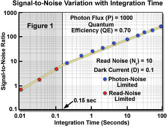
Figure 1 - Signal-to-Noise Variation with Integration Time
Figure 2 - Signal-to-Noise Variation with Integration Time
Because photon noise is an inherent property of CCD signal detection, which cannot be reduced by camera design factors, it essentially represents a "noise floor" that is the minimum achievable noise level, diminishing in relative effect as photon flux increases. Consequently, it is desirable to operate an imaging system under conditions that are limited by photon noise, with other noise components being reduced to relative insignificance. Under low illumination level conditions (assuming dark noise is essentially eliminated by CCD cooling), read noise is greater than photon noise and the image signal is said to be read-noise limited. The camera exposure time (integration time) can be increased to collect more photons and increase SNR, until a point is reached at which photon noise exceeds both read noise and dark noise. Above this exposure time, the image is said to be photon-noise limited.
The limited number of photons available for image formation is a critical factor in many microscopy techniques, and high-performance CCD camera systems are specifically designed to reach a photon-noise limited operation mode at much lower signal levels than conventional cameras, which typically never achieve photon-noise limited performance (and a suitably high SNR) at low light levels. In widefield microscopes, which commonly employ CCD cameras, the total signal available from the specimen focal volume may vary by several orders of magnitude, depending largely upon the imaging technique employed and the specimen itself. A photon flux of 10e6 (1 million) photons per second from the focal volume, an extremely low light level, is equivalent to an average of 1 photon/pixel/second distributed over the surface of a sensor having 1 million active pixels. As a point of reference, the minimum detection limit of the dark-adapted eye is approximately 40 times that (40 million photons/second). A properly designed fluorescence microscope typically yields 10e8 to 10e9 photons per second from the focal volume, or 100 to 1000 photons/pixel/second with the same 1-megapixel sensor. Conventional brightfield imaging mode commonly produces illumination levels, averaged over the full sensor area, of 5000 to approximately 40,000 photons/pixel/second. Unless the integration interval is very short, bright areas of a widefield image can generate a total detected signal of more than 100,000 photons per pixel.
Figure 1 presents a plot of signal-to-noise ratio versus integration (exposure) time for a typical high-performance CCD camera designed for imaging at low signal levels, with photon flux and sensor characteristics fixed at the values shown in the figure. In a plot of this type, a read-noise limited region and a photon-noise limited region can be identified, separated at the exposure time for which photon noise begins to exceed read noise (approximately 0.15 second for the sensor and light flux values specified in the figure). Because of the square-root relationship of photon noise to signal, this division between the two regions occurs at an exposure time for which the total detected signal per pixel is approximately the square of the read noise value. For example, with a read noise specification of 5 electrons rms per pixel, photon noise becomes the dominant noise source when the exposure time is sufficient to result in more than 25 detected photons per pixel at the existing incident photon flux. The interactive tutorial displays a plot similar to that in Figure 1, but reflects changes in the graphical plot as each of the variables controlled by a slider is adjusted. In addition to the calculated SNR value, shown on the left, the right-hand yellow window updates the value ofDetected Photons/Pixel, and the red text message in the upper portion of the graph changes to indicate whether read noise or photon noise predominates for the values selected by the sliders. A red arrow follows the plotted curve as an indication of the currently selected integration time. The transition between the two dominant-noise regimes assumes that dark noise is negligible, which is typical in operation of scientific-grade CCD imaging systems, although other situations are possible. Operation at high dark-current levels alters the significance of the relative values of read noise and photon noise under some conditions, and in such circumstances dark noise can overwhelm both signal and other noise components.
Figure 3 - Signal-to-Noise Improvement with Binning
Some scientific-grade CCD cameras allow implementing an on-chip pixel binning function as another mechanism for increasing signal-to-noise ratio. It should be realized that this method involves a sacrifice of some spatial resolution, as well as a concomitant increase in dark current. By improving the signal-to-noise ratio of the CCD, the imaging system is able to reach photon-noise limited conditions at a lower light level and/or shorter exposure time. Some camera systems automatically utilize a pixel binning mode for monitor display of a preview image to provide a brighter image at rapid frame rates, which facilitates specimen positioning and focusing. To demonstrate this binning effect on calculated SNR, the tutorial provides radio buttons corresponding to three binning factors. The button labels indicate the number of binned pixels as follows: 1 pixel, no binning; 4 pixels, 2x2 pixel array combined into one; 16 pixels, 4x4 pixel array combined into one. Figure 2 illustrates the effect of different binning values on curves plotting the variation of SNR with exposure time. The equation used in the tutorial for calculating SNR is modified to account for binning, as shown below:
Formula 2 - Signal-to-Noise Ratio
SNR = MPQet / [ MPQet + MDt + Nr2 ]1/2
In this modified equation, the symbol M represents the number of binned pixels, and it is assumed that the signal in each of those pixels is the same. The three curves are plotted for the same typical CCD specifications, as denoted on the graph, and for a very low specimen signal intensity, producing a photon flux of 40 photons per pixel per second incident on the sensor. Note that without pixel binning, an exposure time of approximately 4 seconds is required to achieve a photon-noise limited signal level. By implementing 16-pixel binning, an equivalent SNR and total number of detected photons per pixel is reached at an exposure time of only 0.25 seconds (see Figure 2), which would allow refreshing a preview image at an adequate frame rate to permit focusing and specimen positioning even at a low image intensity. Another consideration is that an image acquired using a 4-second integration time would benefit from an approximate 5-times improvement in signal-to-noise ratio with the use of 16-pixel binning, compared to the unbinned mode. In many situations, particularly at low light levels, the benefits of reduced noise and the resulting improved image contrast outweigh the loss of theoretical spatial resolution that is inherent to the pixel binning process.
Contributing Authors
Thomas J. Fellers, Kimberly M. Vogt, and Michael W. Davidson - National High Magnetic Field Laboratory, 1800 East Paul Dirac Dr., The Florida State University, Tallahassee, Florida, 32310.
Related Nikon Products
Share this tutorial:


